Background: Testing PCB Fit Before Sending to Manufacturing
I recently started a project which involved designing a PCB to fit within a very specific enclosure, with tight tolerances and two screws to mount the PCB to the plastic frame. This was designed to fit within an existing enclosure, which I did not have the 3D dimensions for.
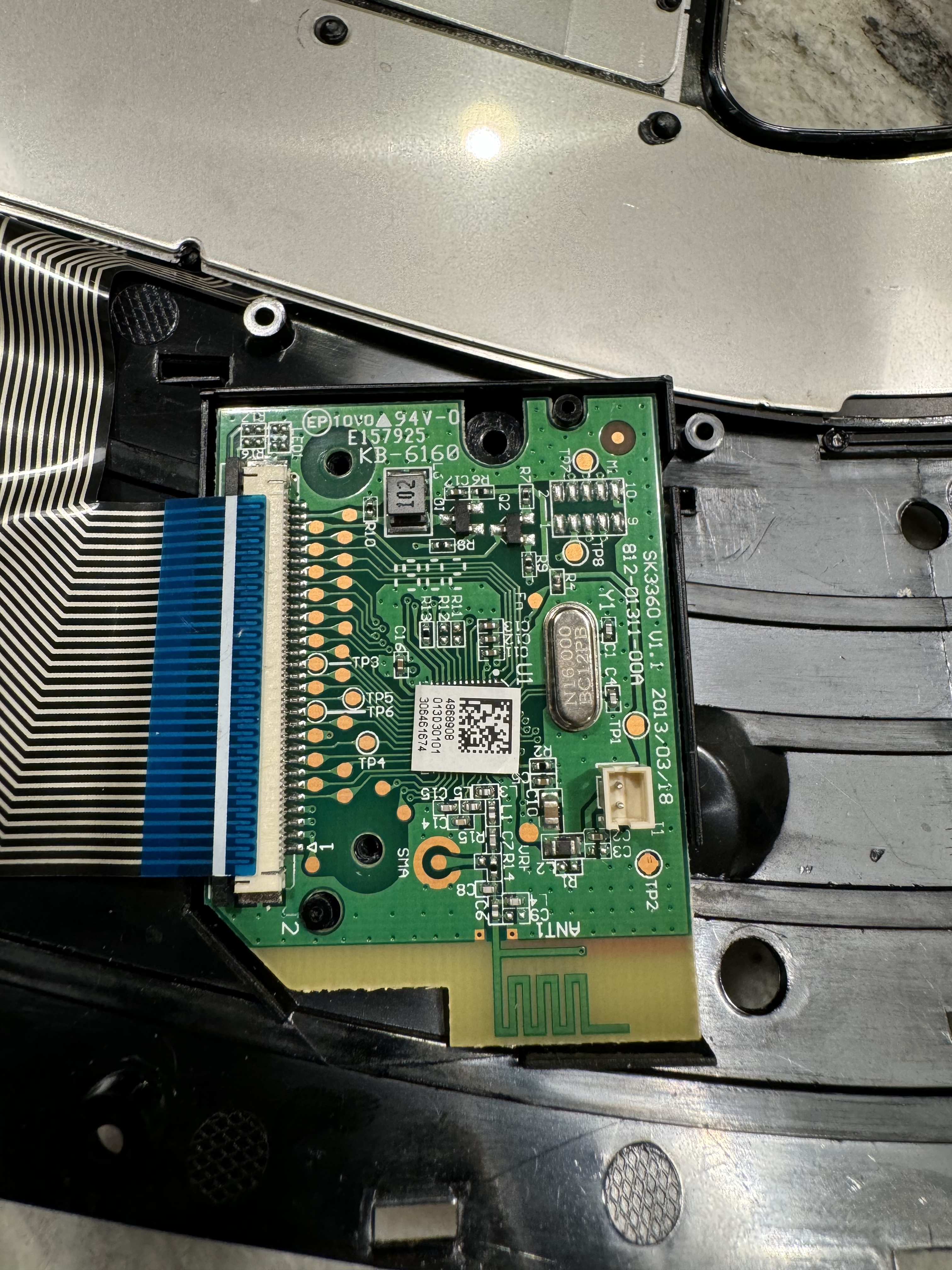
By using my calipers and referencing some open source projects designed to fit within the same enclosure, I was able to make a PCB design outline and mounting holes which I believed would fit. But I was still very hesitant to send it to a PCB manufacturer without performing some test fitting. First I tried printing the design at 1:1 to paper, but I am not the most skilled person with scissors, and I was also concerned that the paper wouldn’t lay flat and wouldn’t be an effective way to ensure good fit.
I then remembered I had a device specifically designed to quickly manufacture parts using computer designs sitting in my home office, an 3D printer. While searching online on how to export from KiCAD (the open source schematic capture / PCB design application I was using) to something PrusaSlicer (the slicing application I use) came up with convoluted workflows (involving OpenCAD, plugins, etc), after a bit of experimentation I quickly realized with the STEP export functionality of newer versions of KiCAD it was exceedingly simple. Since my initial online search didn’t come up with a write up on the process, I figured I’d fill the gap with this quick article.
How to Export from KiCAD into PrusaSlicer
First open the design in KiCAD in the PCB Editor. If you want your parts to show up in the 3D model, make sure the 3D STEP files are correctly imported to where you can see the 3D view of your PCB in the 3D Viewer.
(Steps below are based on Mac, but likely applicable to Windows / Linux as well)
-
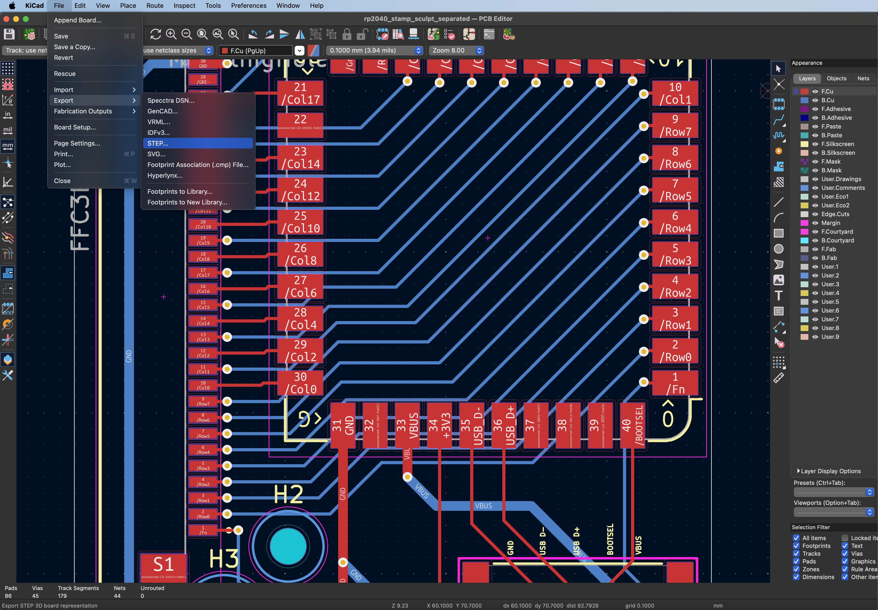
Click File, then Export, then STEP…
-
In the dialog that appears, during my testing
Board Center Originfor Coordinates and selectingOptimize STEP fileworked well. Then click Export.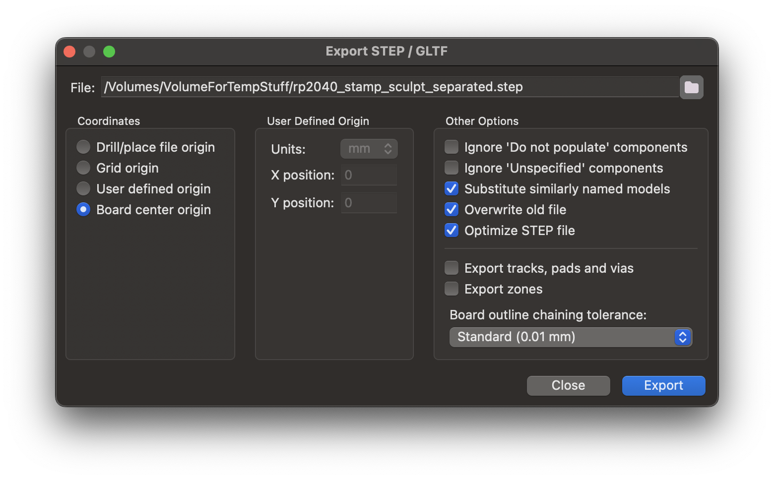
-
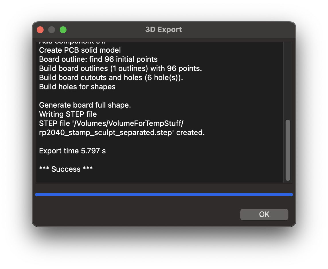
Make sure your export was successful, and take note of where you saved it.
-
Open up PrusaSlicer (or your slicing application of choice), and select File, Import, and the option which includes the STEP file extension.
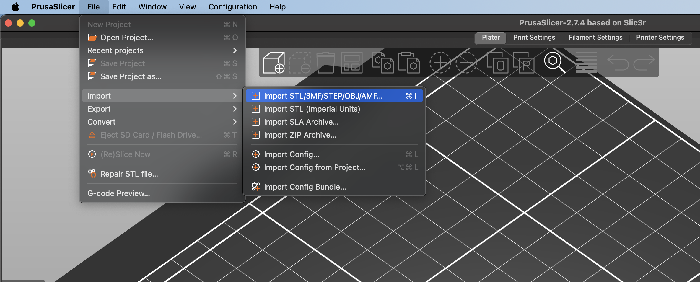
-
Select where you saved the file in step 2, and import it. Note it may take a bit of time to import, even on relatively fast computers.
-
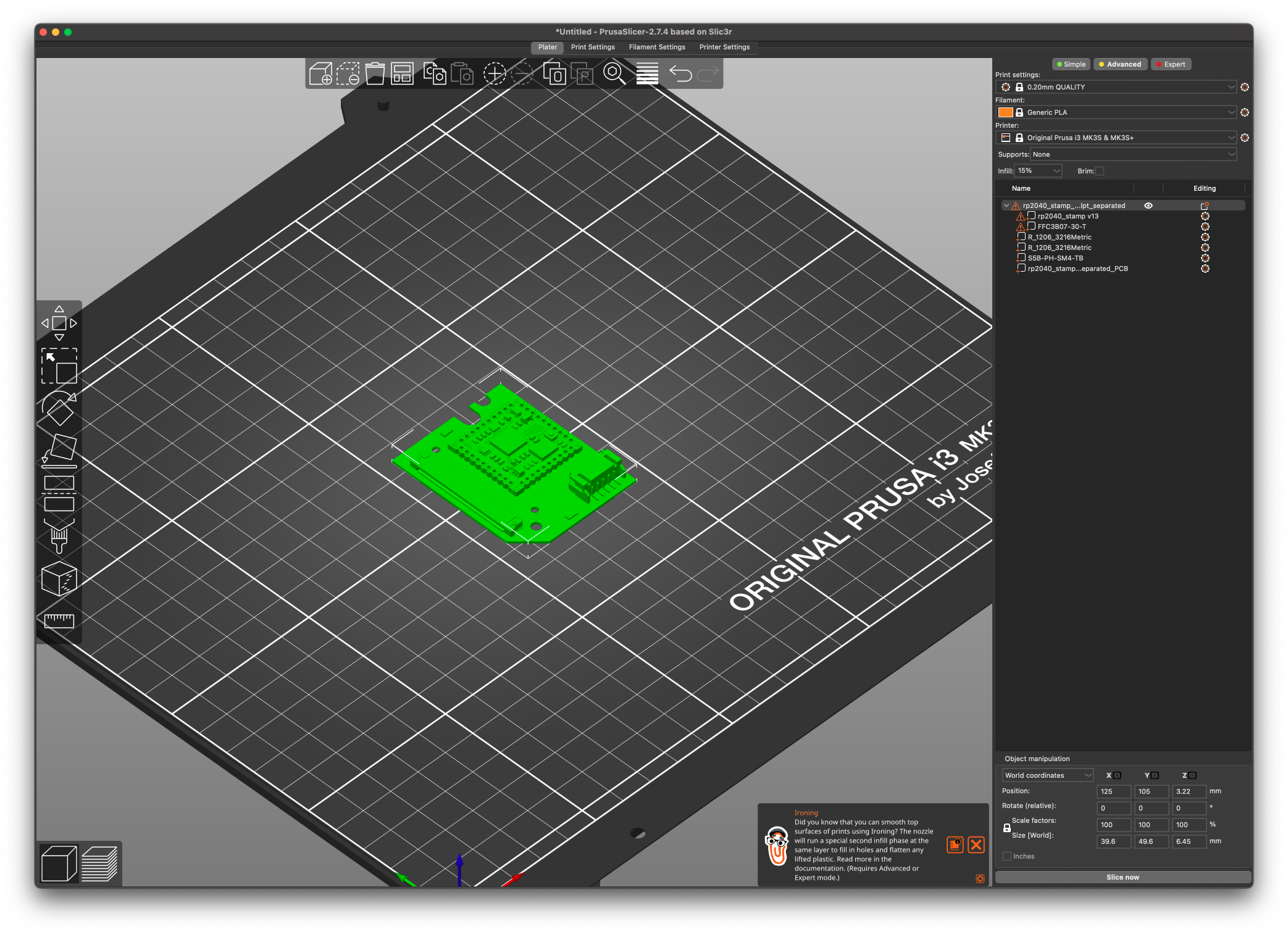
You should now have your PCB design in your slicing application, complete with 3D models of components including SoCs, resistors, connectors, etc! Make sure if you’re 3D printing something with overhangs (like the JST-PH connectors I used on my PCB) you will likely want to go into your
Print Settingsand enableSupport material. If you’re using a recent version of PrusaSlicer personally I prefer using Organic supports. -
Print the 3D model of the PCB, and make sure it fits!
Test Fit Success
After a couple 3D prints as I adjusted elements of the PCB (including adjusting the ribbon connector down from where I initially placed it), I felt I had a design which fit correctly onto the plastic enclosure.
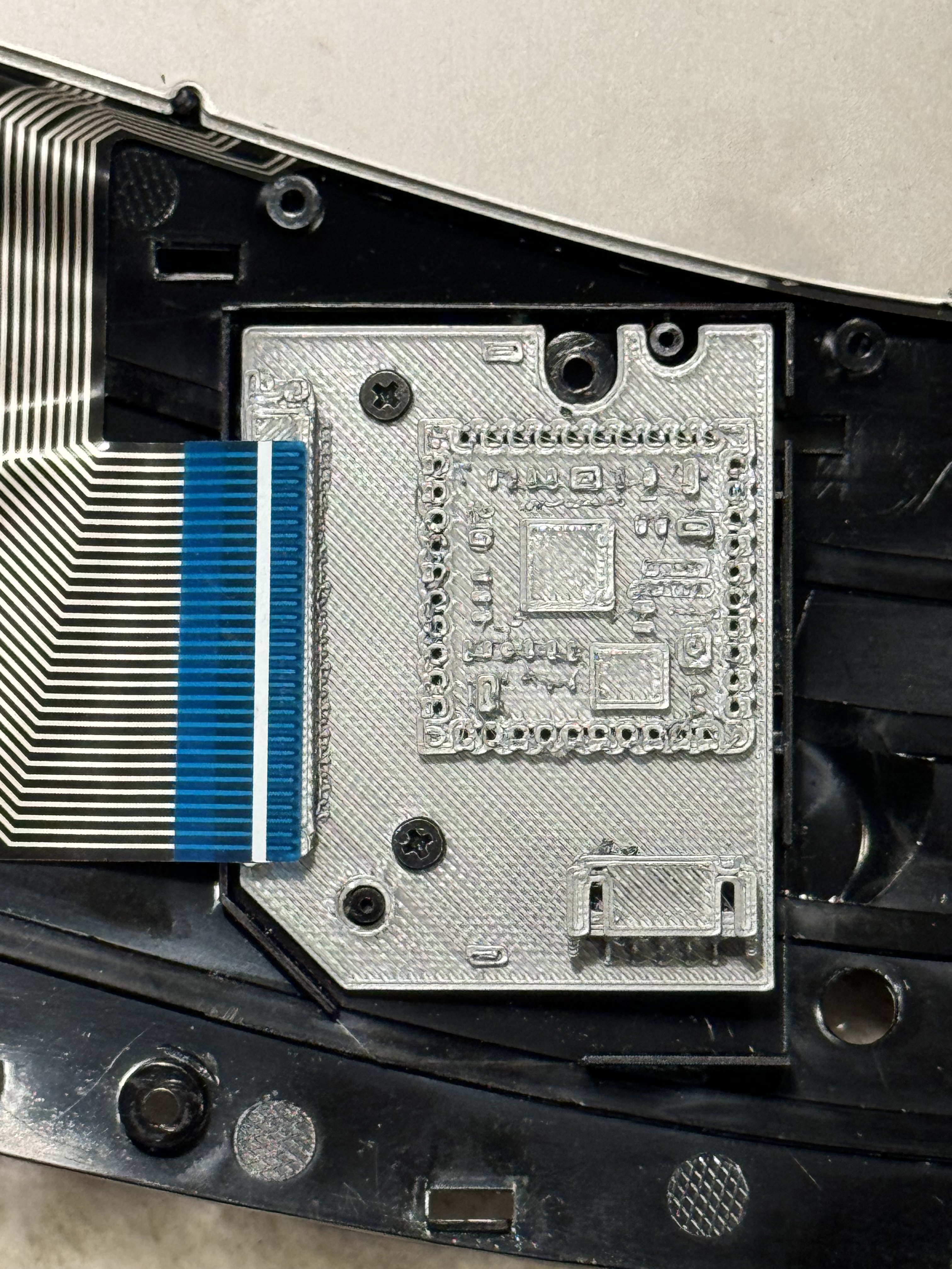
This gave me a lot more confidence to then send the design out for PCB manufacturing and assembly.
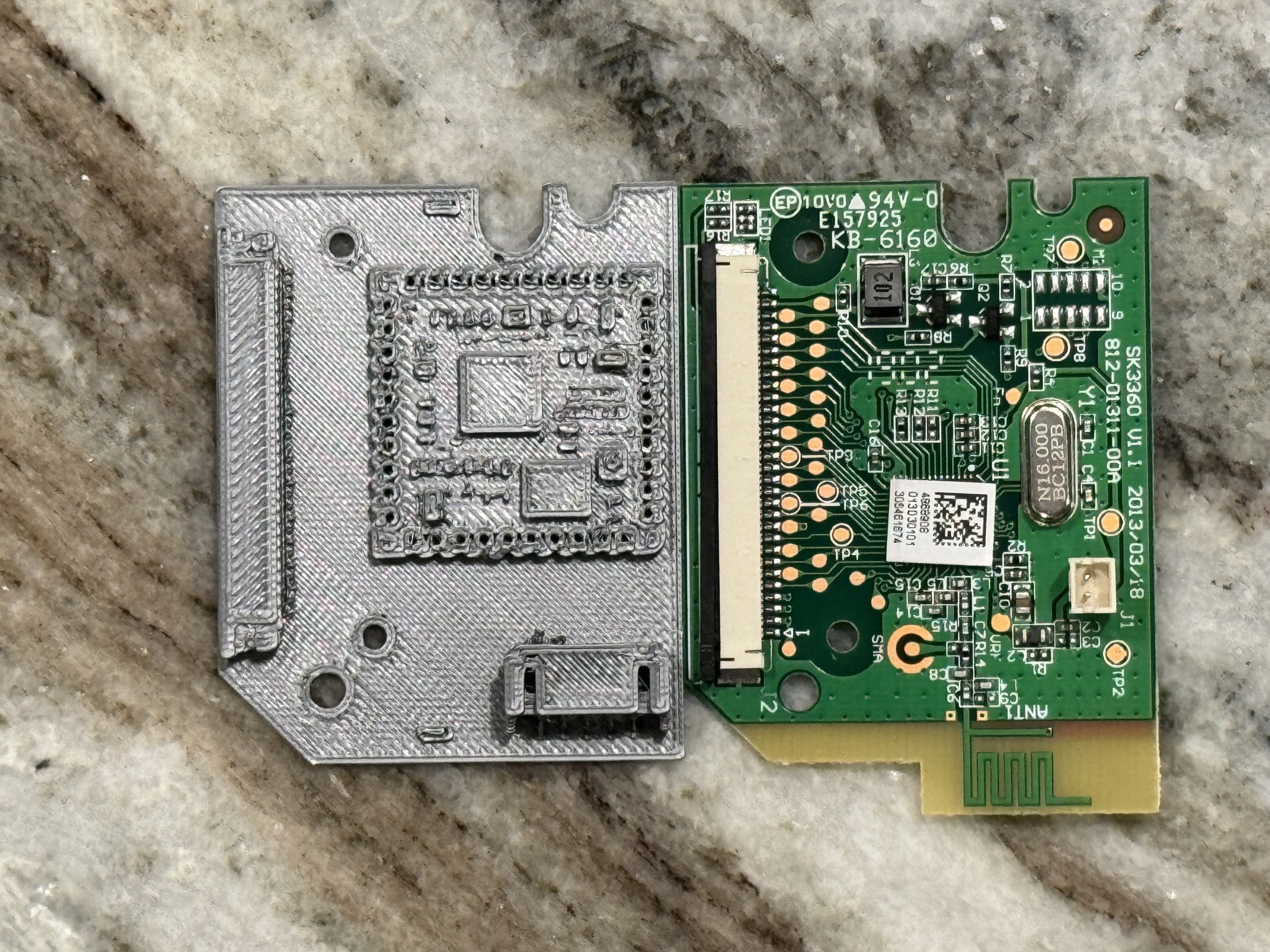
A Perfect Fit on the First Revision of Manufactured PCBs
Once the PCBs came in, I was estatic during the first test fit to see they fit perfectly.
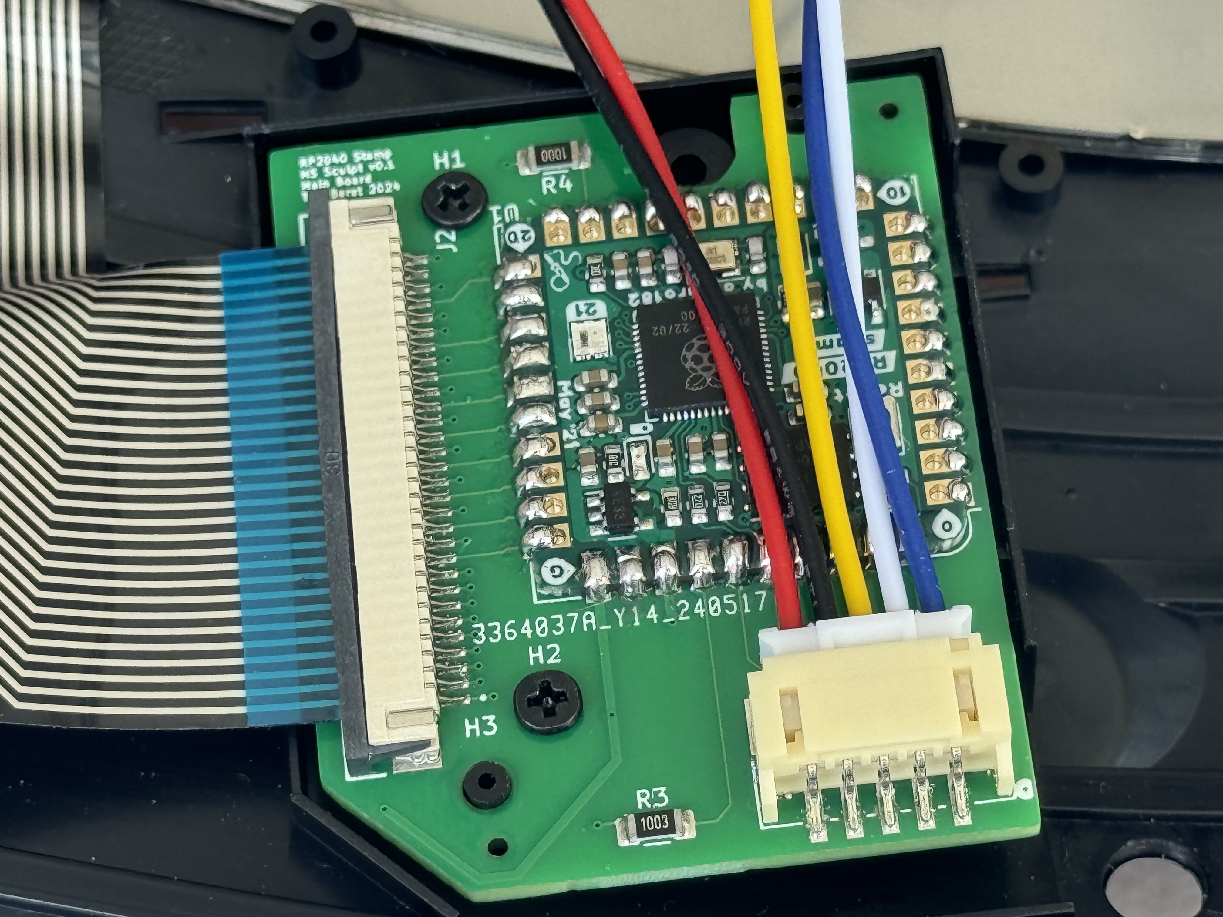
The fact that my first assembled PCB design fit perfectly I attribute at least partially to having 3D printed multiple versions of the board, and being able to test fit before even bundling the KiCAD outputs to send to a PCB manufacturing and assembly house for quotation.
More to come on this project, once I get an opportunity to properly write it up. My apologies about the quality of the images in this post, they were just off my cell phone because I didn’t think to stop and get proper photos with my “big” camera during the early phases of it.