Table of Contents (apologies, this is a long post)
- My Favorite Keyboard: The Microsoft Sculpt Ergonomic Keyboard
- Microsoft Stops Production of the Sculpt, Evaluation of Logitech K860
- Sculpt PCB Replacement to the Rescue?
- Raspberry Pi Pico Proof of Concept
- Time to Design a Real PCB!
- How to read the Fn switch?
- KiCad
- Where to order?
- Getting the first units back from assembly
- Final Assembly
- Improving the underside of the Sculpt
- A keyboard I’m loving
- Appendix A: The cost
- Appendix B: Project Source Code Links
- Thanks for reading!
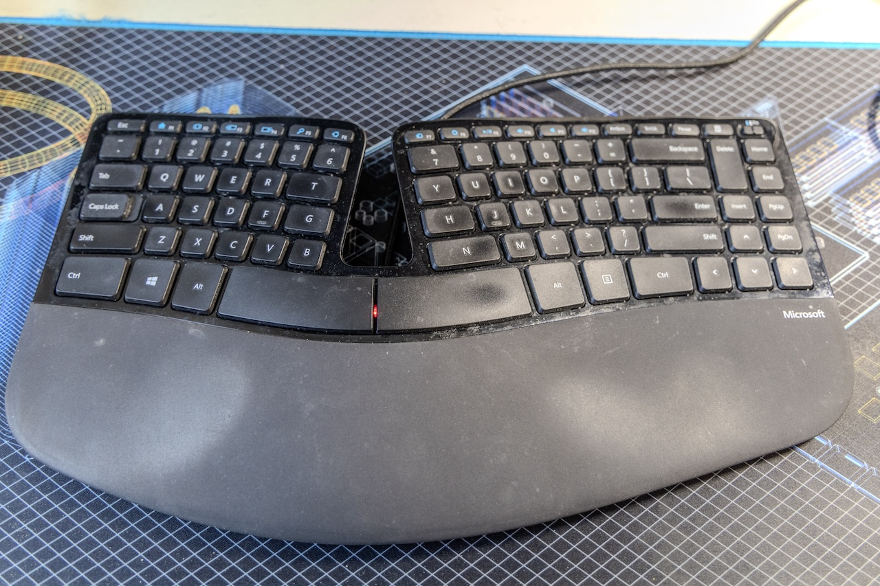
My Favorite Keyboard: The Microsoft Sculpt Ergonomic Keyboard
As a young child, I realized that I would likely be using keyboards for the rest of my life, both professionally and for entertainment (gaming). I recall seeing the original Microsoft Natural keyboard and how it was designed to reduce the likelihood of repetitive stress injuries. I purchased one used as a pre-teen, and adopted to a split keyboard layout.
Throughout the years I have transitioned multiple times to newer Microsoft Natural keyboard generations. I eventually settled on the Sculpt Ergonomic as my preferred keyboard I believe in 2014.
The Sculpt Ergonomic kept the split keyboard layout I’ve used the majority of my life, and also featured low-profile chiclet keys that reminded me of the better Apple laptop keyboards that I have used.
But it had issues…
While the Sculpt was my favorite keyboard, it definitely had some flaws. Most annoying was the fact that it used a permanently paired wireless dongle to communicate with the keyboard. The keyboard and dongle used a proprietary communication protocol, and as such if you ever lost the dongle you effectively had a paperweight. This issue is big enough it warrants a mention in the product’s wikipedia entry.
Another annoying trait was the keyboard would go to sleep after some time elapsed without a key being pressed, and miss the first key or two after you woke it from sleep.
More annoyingly for me, the keyboards had some RF issues which seemed to get progressively worse the older the keyboard was. At my work I had a habit of using a USB extension cable and then having the dongle sit directly between the split gap in the middle of the keyboard. Even with these workarounds, usually 6-12 months after purchase the dongle communication would get so intermittent and drop enough random keystrokes I would purchase a replacement keyboard. I just considered the $60 periodic purchase price a cost of having a good keyboard to write code, documents and game on.
Microsoft Stops Production of the Sculpt, Evaluation of Logitech K860
I was extremely concerned when I saw the headline last year that Microsoft was going to stop producing most of their peripherals, including my keyboard. I purchased two spare keyboards, figuring that would at least give me time to figure out a replacement.
I tried the Logitech K860 (Amazon link), which featured similar looking keys and a good split. It also had nice features like both standard Bluetooth and custom Dongle support, and the ability to configure certain profiles to have flipped Alt/Win key profiles (useful for using non-Apple keyboards in MacOS). But I overall didn’t love the key feel, and more importantly strongly disliked the additional separation between my keyboard and mouse having an attached number pad created. I didn’t realize how accustomed I had become to having my mouse directly next to my keyboard with no numpad in between.
I tried a couple additional ergonomic keyboards at various stores, but none of them matched the overall feel of the good ol’ Sculpt.
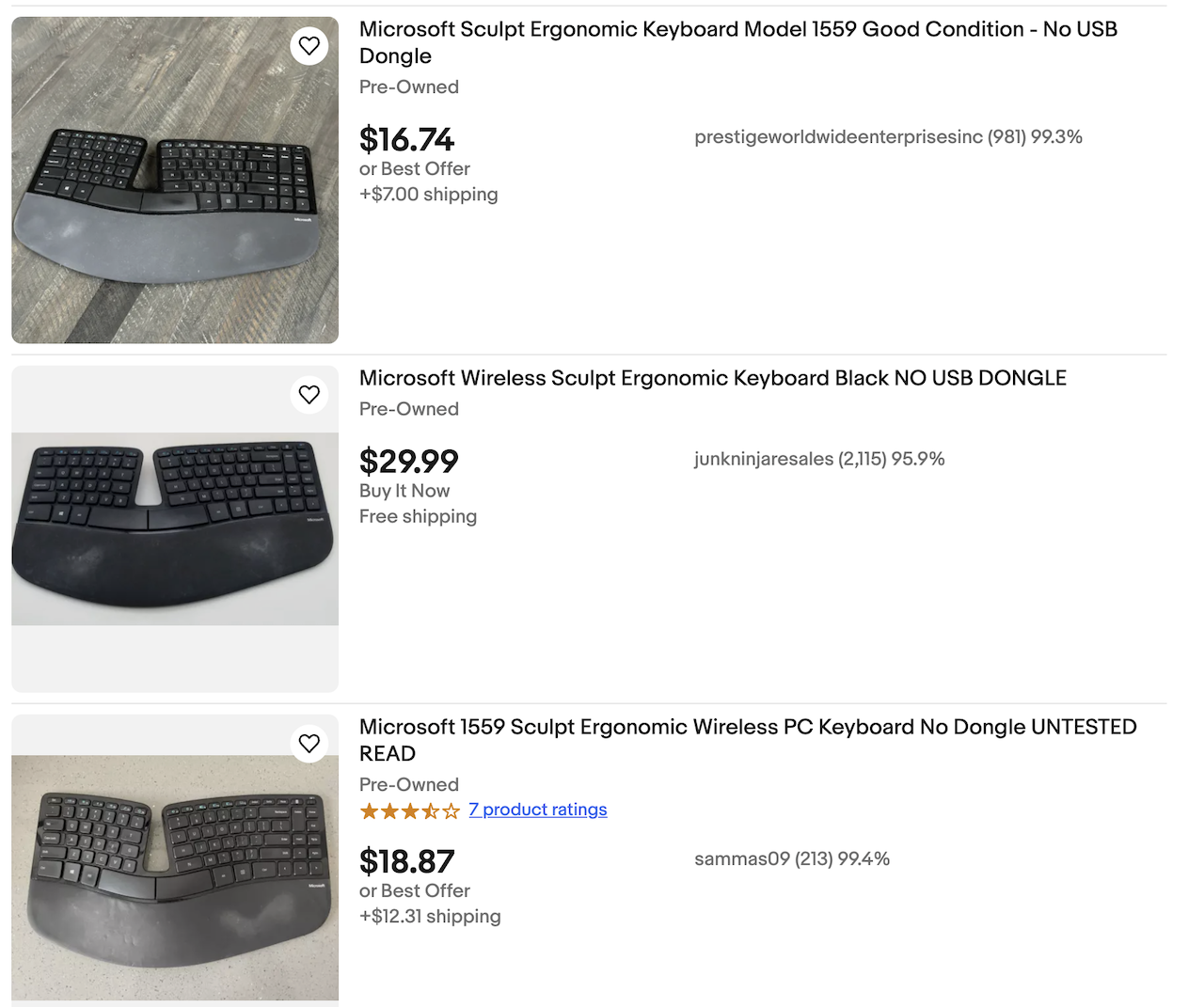
Sure enough a couple months after Microsoft stopped production the keyboards had skyrocketed in cost. Whereas I previously was able to order them for ~$60 from Amazon, they were now fetching $300-$400 new from resellers (cough scalpers cough).

I was entirely unwilling to give a scalper a ton of money for a keyboard.
So that raised an important question: Would I be forced to use a keyboard I didn’t prefer, or was there another option that would allow me to continue using the Sculpt?
Sculpt PCB Replacement to the Rescue?
A couple years ago I had read about people who had replaced the PCB in the Sculpt Ergonomic in order to address some of the flaws in the keyboard.
There are a couple of Sculpt PCB projects I want to call out as being very helpful as I began my own journey to having a custom PCB nestled within my beloved Sculpt Ergonomic:
-
Chris Paynter: Modding the Microsoft Sculpt Ergonomic keyboard to run QMK (and make it wired)
This writeup was incredibly helpful, particularly the ordering of the different pins on the ribbon connector.
-
Microsoft Sculpt Wired Conversion Mod
A phenomenal writeup and awesome first-time PCB design. His writeup provided critical data, particularly the configuration of the
Fnswitch and the unexpectedly complex wiring of the LEDs.
This raises the question of why I didn’t just use one of the PCBs linked and open sourced in the above projects. The simple answer is I had my own set of requirements:
- Don’t leave any potential performance / features on the floor (within reason).
- In my opinion this ruled out the PCB design used by Chris Paynter, as it merged the Right Shift and Right Alt into one column. With the fact that the Sculpt doesn’t use diodes to better isolate keys, I was worried this would potentially cause spurious or missed reads if I had two people using the keyboard for a game. I might have been being paranoid, but this design also violated requirement 2.
- The reason I included the (within reason) is while I wanted to enable features, I also didn’t want to go overboard with my first rev. For example I decided to not worry about the second LED on my first hardware rev, which would have required either a inverting charge pump or an IC supporting negative voltage output. See Chad’s writeup for more details on the wiring setup of the LEDs.
- No external keyboard modifications required (e.g. no Dremel / cutting keyboard) if at all possible.
- Considering that the number of Sculpt ergonomic keyboards are currently finite (at least until Incase begins manufacturing their new line), I didn’t want to be cutting into the keyboard. I was initially concerned this wouldn’t be possible, but figured out a way.
- Use only in production parts.
blttll’s PCB design uses the Teensy 2.0, which is no longer being manufactured, which ruled it out.
- The keyboard should interface using USB-C. And make sure it works plugged in either direction.
- Almost everything is moving to USB-C. I want my keyboard to use it as well.
My next question was whether I wanted to modify an existing design, or implement my own from scratch. In short I decided to design it from scratch, leveraging an MCU that was guaranteed to be in production for an extended period of time.
This decision was driven by wanting to have ownership over my design, and using it as an opportunity to do a more complex (at least for me) PCB design.
A Thriving “For Parts” Market on eBay
While I had a stash of two old keyboards which had partially failed, that wasn’t going to be enough for my long term usage or even potentially this project if I damaged some. I also didn’t want to potentially sacrifice an even partially working keyboard for my testing.
I hit up eBay, and was able to acquire some old Sculpt Ergonomic keyboards with missing wireless dongles for relatively cheap (less than $30 including shipping per keyboard). Note that you do need to be careful, as there are some which are in poor condition. The fact some eBay sellers seem to have point and shoot cameras from the early 2000s also makes it difficult to evaluate condition.
The Processor Selection
With how frequently MCUs seem to come in and out of vogue / availability nowadays, for this project I decided I wanted to select one that would be around for a while. I also had a number of requirements.
- Support for the QMK keyboard firmware.
- QMK is an open source keyboard firmware for AVR and some ARM USB family chips. It is extensively used within the maker community for custom keyboards, and even some manufactured ones. It is also the firmware used by some of the previous custom Sculpt PCB projects. Since I didn’t want to build a brand new keyboard firmware, I wanted to use a processor fully supported by QMK.
- Minimum 29 GPIO pins (independent of flash / USB support).
- The ribbon cable coming from the main portion of the Sculpt keyboard has 30 pins. One is the ground which can electrically tie into the ground plane of the MCU, so that means we require at least 29 GPIO pins.
- Ideally a module for the processor exists which includes most of the “supporting” chips to make the initial design easier.
- I was extremely impressed by how Chad Austin went from 0-60mph on his first design. That being said this would be my first medium complexity layout, and I wanted to use a module that had most of the supporting chips for the MCU already built in. This would dramatically the complexity of my layout and reduce my PCB component count.
- Fits on a PCB within the existing Sculpt PCB footprint.
- There are size constraints to operate within. While not as tight as some work projects I’ve worked on with professional EEs, it definitely was the smallest PCB layout I had worked on for a personal project.
- Extended manufacturing support lifetime.
- See #3 in project requirements section.
Requirements 2 and 4 instantly removed a bunch of the existing chips. For example, the Teensy line either didn’t have enough pins or were too large to fit within the Sculpt PCB footprint. #5 also ruled out some older MCUs.
Looking over the list of QMK supported processors, the RP2040 caught my eye. While the Raspberry Pi Pico board did not fit within the size or GPIO count constraints, after a bit of searching I discovered the RP2040 Stamp.
The Stamp looked perfect for my use case. It had virtually everything you needed integrated onto a single solderable component, exposed every GPIO pin the RP2040 had, and was small enough to fit on my PCB. It also was specifically designed to be hand solderable to a PCB.
Even after selecting the RP2040 Stamp, I didn’t want to try and move forward without developing a proof of concept for the RP2040 on the Microsoft Sculpt. So I ordered a Raspberry Pi Pico, a Pico breakout board, and a ribbon breakout board for the 30 pin 1.0mm Sculpt ribbon cable.
Raspberry Pi Pico Proof of Concept
The First Disassembly
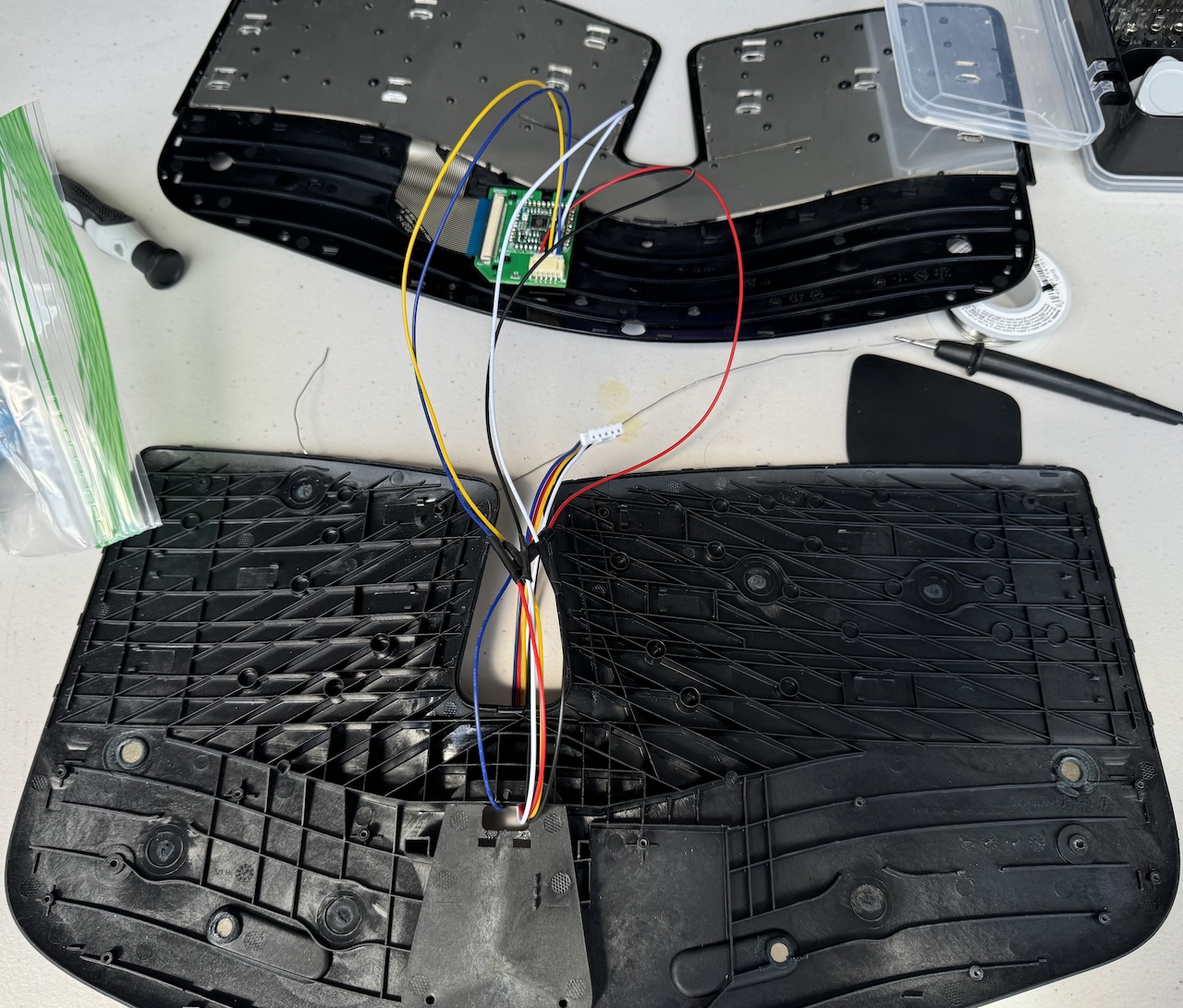
Before I could try installing the proof of concept, I needed to disassemble a keyboard. I grabbed a mostly dead (periodic key drops, even with the dongle directly below the keyboard) Sculpt from my stash. I intentionally picked one that was relatively beat up as well. I then began following the instructions online on disassembling the Sculpt. A short while later, I had a keyboard disassembled enough for me to remove the existing PCB.
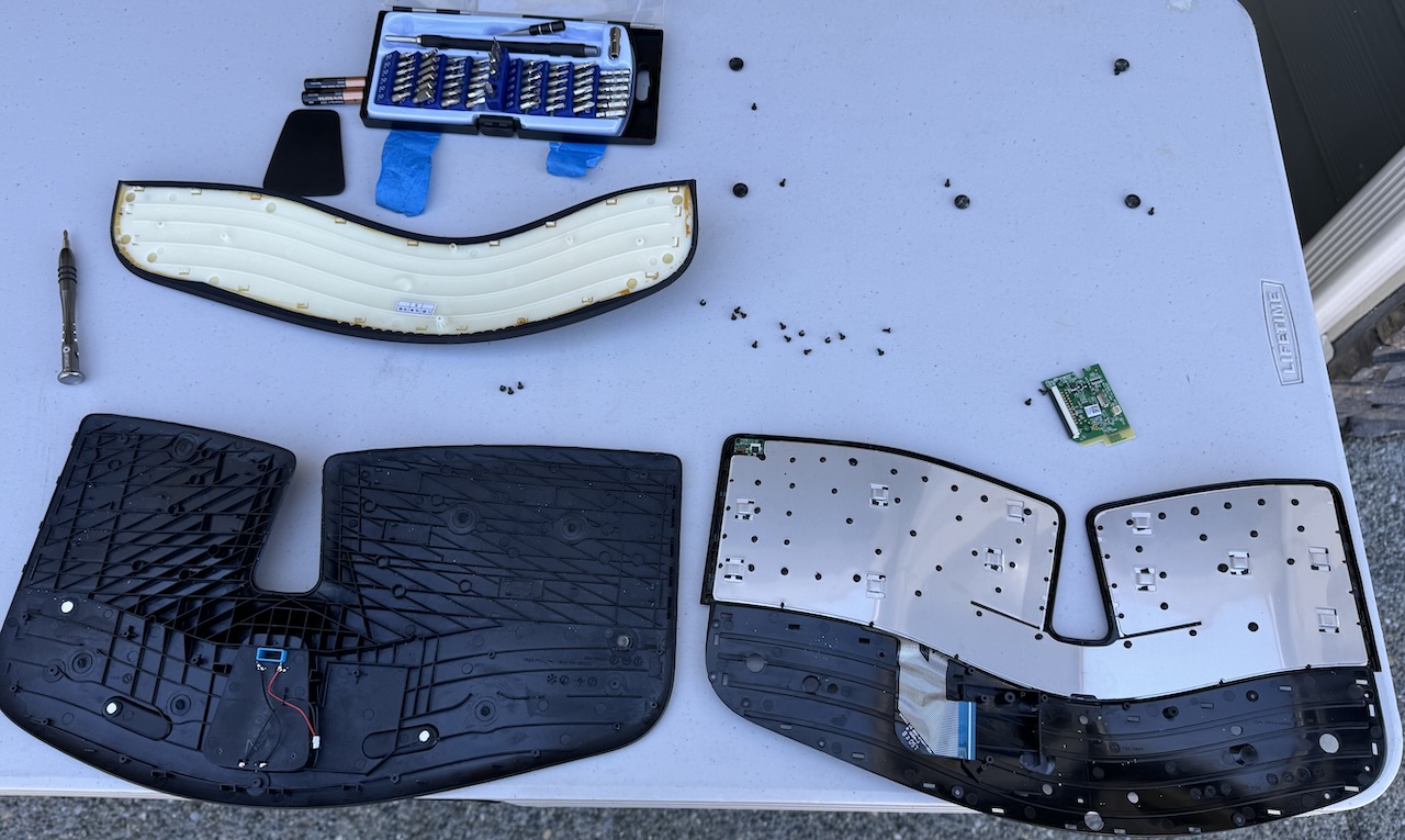
You can see the stock Sculpt PCB sitting atop my folding table just above the disassembled half of the keyboard on the right.
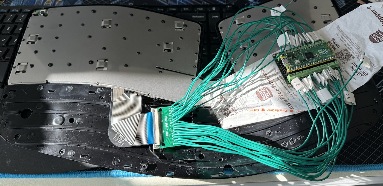
First RP2040 <-> Sculpt Testing
After a bit of soldering wires to the 30-pin breakout board, code modification, and hand wiring, I was ready to test out whether the Microsoft Sculpt would work correctly with an RP2040 (running on a Raspberry Pi Pico).
Amazon link for Raspberry Pi Pico breakout board
I didn’t have enough GPIO pins on the Raspberry Pi Pico to connect everything coming from the ribbon cable breakout board, so I didn’t worry about hooking up the LEDs or Fn switch. I also merged a couple of the lines together where possible based on the keyboard map. This wasn’t something I was willing to do for the final project, but for the proof of concept it was fine.
After hooking everything up, I plugged the keyboard into my laptop and anxiously waited as the QMK firmware using my proof of concept keyboard layout configuration compiled and flashed onto the RP2040. After the automatic power cycle I was excited when Mac OS came up with the new keyboard detected dialog. After pressing a couple keys (which were detected!) to pass through the keyboard layout detection, I opened a new file in VS Code and began typing.
The keyboard worked! Woot!
Until I tried to press some of the function keys…
A bunch of other characters were included with each function key press. At first I was worried I had crossed some of the wires or misconfigured the keyboard layout, but then realized it was because I was causing the metal back plate of the keyboard (which was entirely disassembled, as there was no way I was going to fit the rats nest of wiring through the battery hole at that moment) to impact against the Raspberry Pi Pico pins when I pressed the upper keys.
A quick electrically insulating layer later (yes, that is a paper receipt between the Pico and the keyboard), and I was able to use an online key checker to verify that all the keys were working.
Time to Design a Real PCB!
After the euphoria of the prototype having worked passed, I knew the next step was to design something that could be reassembled into something resembling the original keyboard.
The first open question I had was how I wanted to attach the keyboard to my computer.
While my original draft PCB schematic was on a single PCB (assuming I would have to dremel like everyone else), as I worked on the design I had the idea of splitting the layout into two parts. One half would be installed in the existing space allocated to the original PCB in the Sculpt, and would have basically everything except for the USB connection. I would then use a very thin cable to route between the “internal” PCB and what I deemed the “interface” PCB, which would be installed into the existing battery slot.
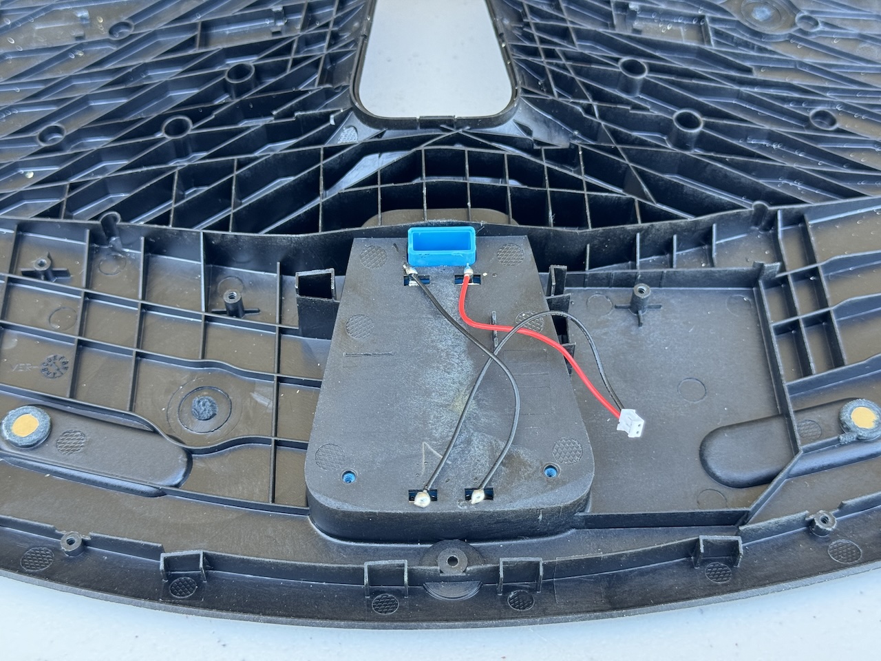
By removing the plastic battery holder, I could likely fit very thin wires taking a similar path the stock battery wires took from the internal PCB to the battery compartment, where I could mount my USB-C interface PCB.
Routing cables…
More constricting for my design than the hole (which is large enough to shove a USB-A connector through) was the gaps between the mounting location for the PCB and the lower portion of the keyboard were incredibly narrow. There was no realistic way you could route a USB cable in between the PCB location and the USB dongle hole, outside of perhaps a super thin one.
I looked into connector standards used for embedded applications, and came across JST connectors. They were widely used in custom drones, and supported cables with very small diameters. I decided the JST-PH connector’s supported more than enough current capacity, and was still likely thin enough for my project.
How many wires do you need?
A keyboard doesn’t need much speed. In fact the RP2040 (my chosen MCU) only supports USB 1.1 (11Mbps maximum). For standard USB (1.1/2.0), you only need two pins for data: D+ and D-.
For power, we need a ground and a 5V input line.
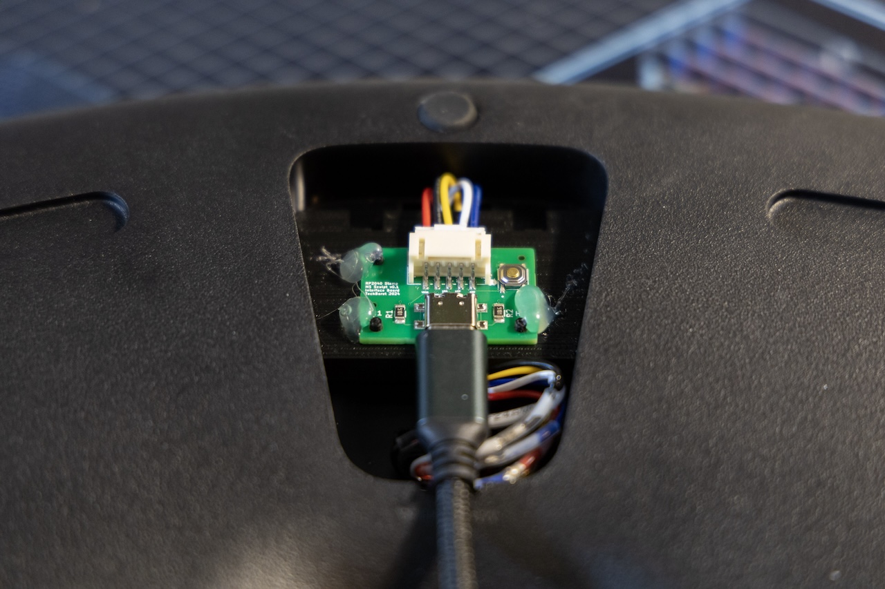
I decided for ease of use I wanted to break out the RP2040’s BOOTSEL pin, which allows you to force the RP2040 into a mode where you can flash the board. After dealing with overly complex boot loader schemes for various dev boards, I find the RP2040’s design simple and rather clever, as the RP2040 will then appear as a standard USB mass storage device when started with BOOTSEL pulled to ground. By copying a firmware file you can overwrite the current firmware, and the RP2040 will automatically restart into the new firmware.
So that meant I needed to pass the BOOTSEL out to the user-accessible PCB, via a button.
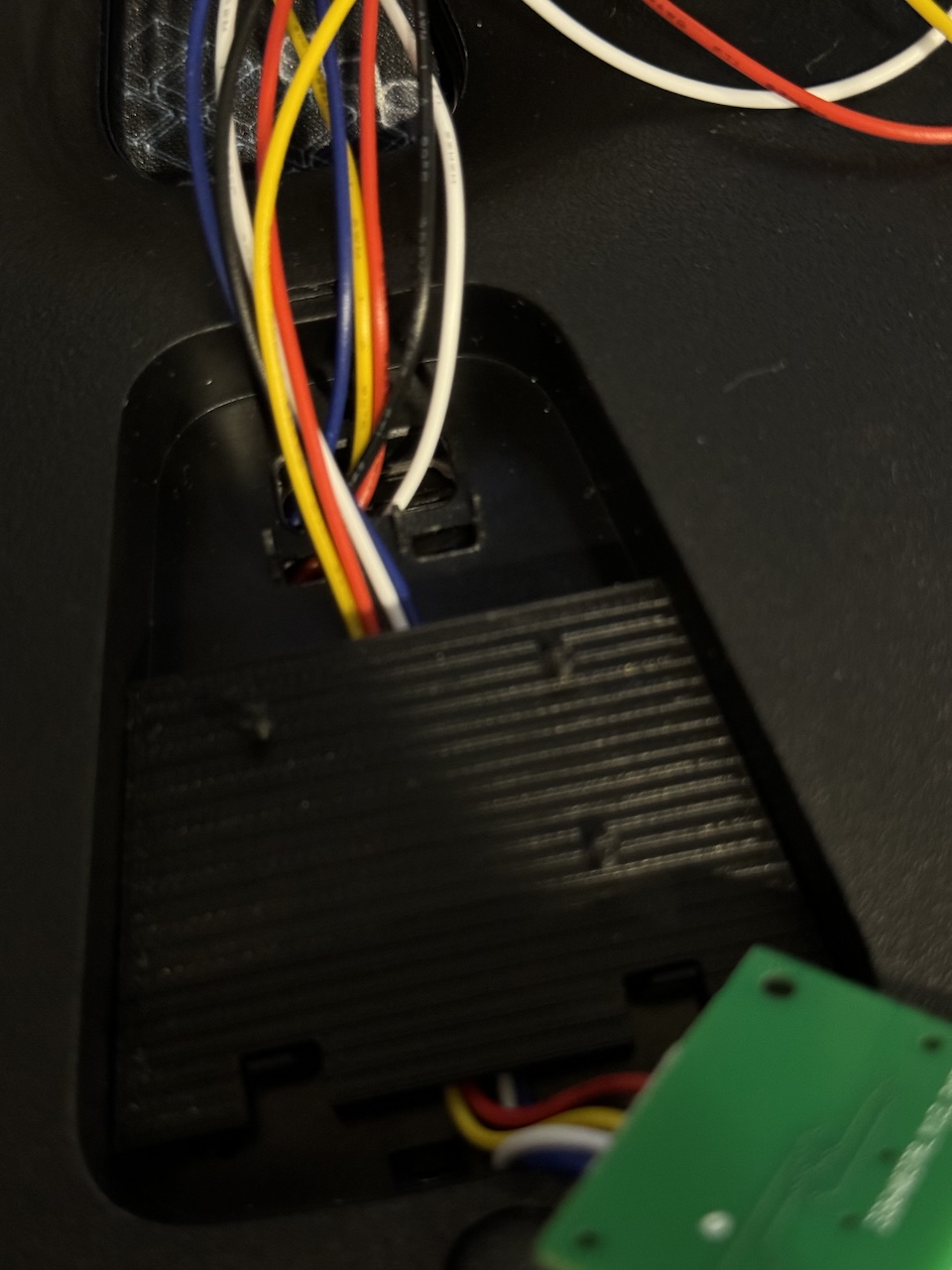
Summing everything above up, I need a total of five wires passed between the two PCBs: Ground, 5V (Vin), D+, D-, and BOOTSEL.
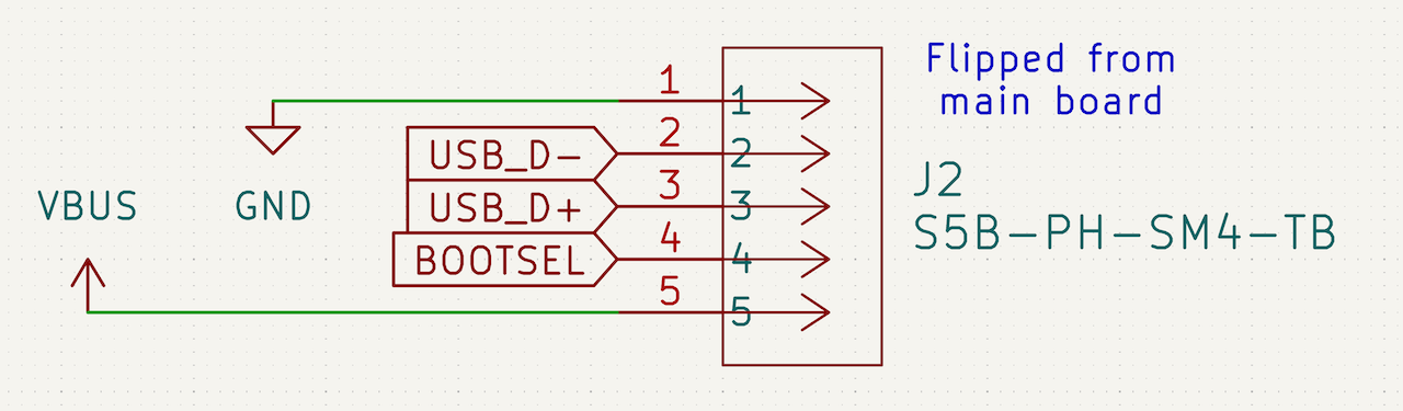
I used some pre-manufactured JST-PH cables (Amazon link) with male connectors available on Amazon. I had read some horror stories about trying to crimp your own JST cables, so I decided I didn’t want to worry about it for this project.
I wasn’t worried about needing to solder the two cables to make a male<->male JST-PH cable.
In looking up USB-C specifications I learned that for the keyboard to be detected as a 5V device I needed to place 5.1K ohm resistors between CC1 and ground, and CC2 and ground. Similarly in order to have the connector be orientation-independent I needed to tie DP1 and DP2 together, and DN1 and DN2 together.
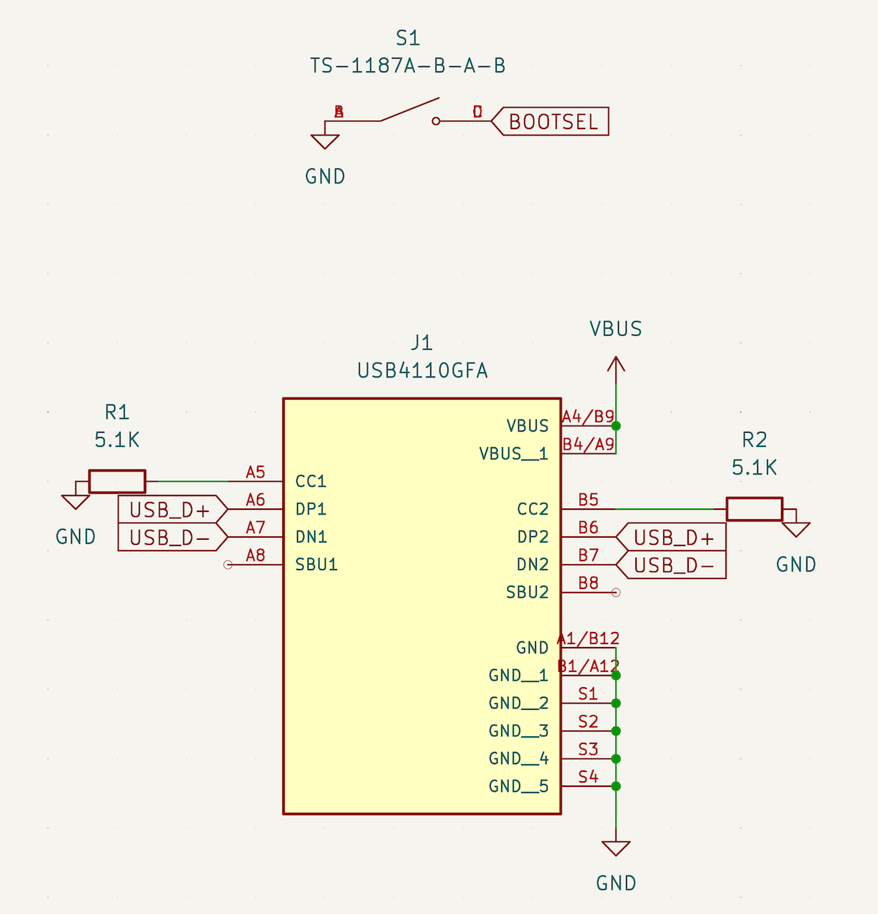
How to read the Fn switch?
The next small challenge I faced was the Fn switch, which changes whether the function row acts as function keys or multimedia/etc keys. As detailed in Chad Austin’s project writeup, the Fn switch acts like a switch changing the value of a resistor between the Fn pin and ground. So effectively if you applied voltage to the Fn pin, the Fn switch would vary a resistor between Fn and ground between either 47K ohm or roughly half a megaohm (500K).
This called for a voltage divider.
By putting a resistor of a specific value between Fn and Vin, I could then read the voltage value of Fn and based on the voltage value read determine if Fn was set to a high or low resistor value. I ran through the math on a couple common resistor values, and liked what I saw using a 100k ohm resistor. Since the RP2040 stamp had a regulated 3.3V output I decided to use it instead of the 5V VIN, both because it would likely be more stable than the 5V coming through the tiny JST-PH cables, plus it would reduce overall power draw.
| Fn Switch Setting | Fn resistance (Ω) | Total Fn Circuit Resistance (Ω) | Fn Voltage (3.3V input) | Fn circuit current draw (µA) | Fn circuit power draw (µW) |
|---|---|---|---|---|---|
| Low | 47k | 147k | ~2.24V | ~22 | ~72 |
| High | 500k | 600k | ~0.55V | ~5.5 | ~18 |
The large delta in values gave me some confidence that the RP2040 would interpret half a volt as a low signal and the roughly 2.24V as a high signal. I was able to confirm this using a quick test with a Raspberry Pi Pico, variable power supply, and CircuitPython.
KiCad
KiCad has become somewhat universal in the open source community for circuit design. I tried to use it a number of years ago for the previously mentioned extremely simple PCB layout project, but ended up switching over to Fritzing because it allowed me to quickly get the project laid out instead of needing to learn a new application. Now I needed the power KiCad could provide.
To start off, I watched a couple YouTube tutorials about KiCad. I found the sequence of videos where a DigiKey creator designed a RP2040 based PCB had a nice alignment with my project, and helped me learn a number of things to watch out for.
I then began working with KiCad, and first thing I needed to do was get the RP2040 Stamp schematic, footprint, and 3D layout imported correctly.
Kandle (KiCad Component Handler) makes component imports FAR easier
KiCad’s library management was not great, or at least I wasn’t finding the right documentation to guide me through the process.
After struggling for far too long to get the RP2040 Stamp files to import correctly into my project, I spent some time Googling and reading and came across an open source project dedicated to automatically importing components into your project, including the symbol, footprint, and 3D model libraries. Kandle unblocked me, and I tip my hat to the author for making a great project solving a problem that was frustrating me and I’m sure lots of other engineers.
I imported in all the external components I needed, including the JST connector, ribbon cable connector, and most importantly the RP2040 Stamp.
Lack of KiCad Support for Multi PCB Projects
One frustrating thing was that after searching online it looked like the only way to have multiple PCBs in KiCad was to have multiple projects. So my Sculpt PCB project was separated into two different KiCad projects: rp2040_stamp_sculpt_separated (main board) and rp2040_stamp_sculpt_interface (USB interface board).
A Design I’m Proud Of
Even after I got the parts imported, I went through multiple trace layouts before I got one I was proud of. By alternating between the distant and close pins I was able to design a layout with a small number of layers (2) and whose traces didn’t look like a horrible rats nest.
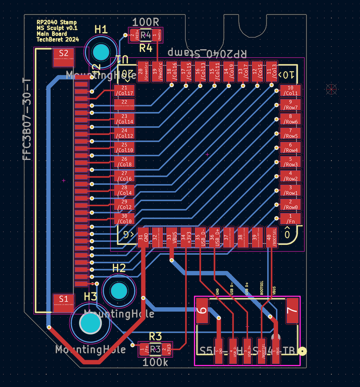
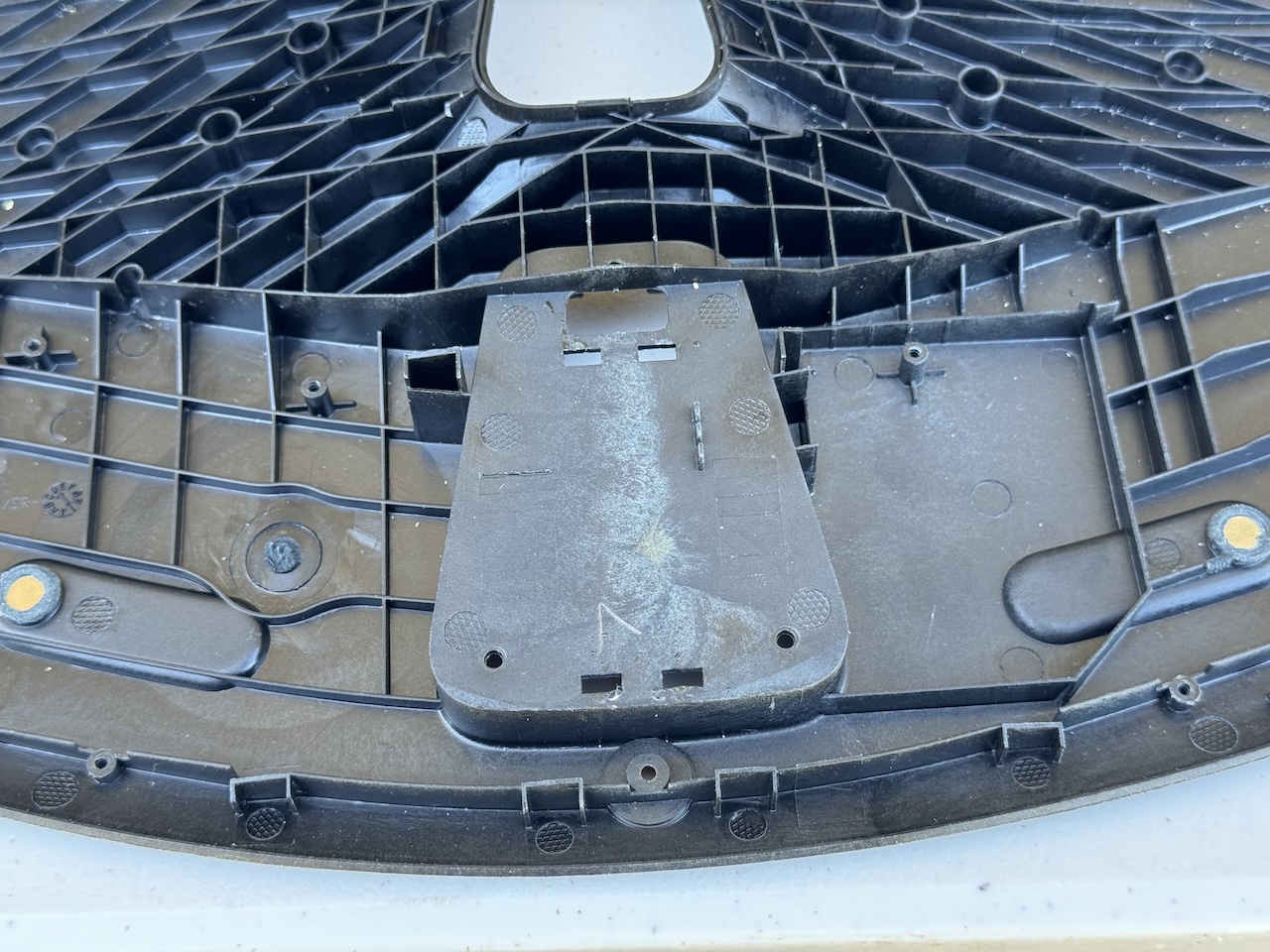
You can see above the layout of manufactured version of the main PCB (the one which hides inside the Sculpt).
3D Printing allows for fit test prior to manufacturing
I wrote a separate blog post about how to convert from a KiCad 3D project into a 3D print. I was surprised it wasn’t discussed online more, as I could see this being invaluable, particularly when you’re trying to interface with physical components that you don’t have a 3D model for, and so are going off of manual measurements or even worse rough estimates.
3D printing the 3D PCB model, complete with 3D representations of the soldered components let me perform a test fit and make sure that it screwed down onto the slot. It also allowed me to check where the ribbon cable was in relation to my connector, and in fact prompted me to adjust it slightly to better align it with the physical cable’s location. It also helped me realize I had selected the wrong hole size for one of my mounting holes, which would have mandated another revision. So the less than a dollar worth of plastic I used likely saved me $50+ in not needing another set of PCBs manufactured.
Below is a photo of the original Sculpt PCB sitting next to one of my 3D printed PCB models
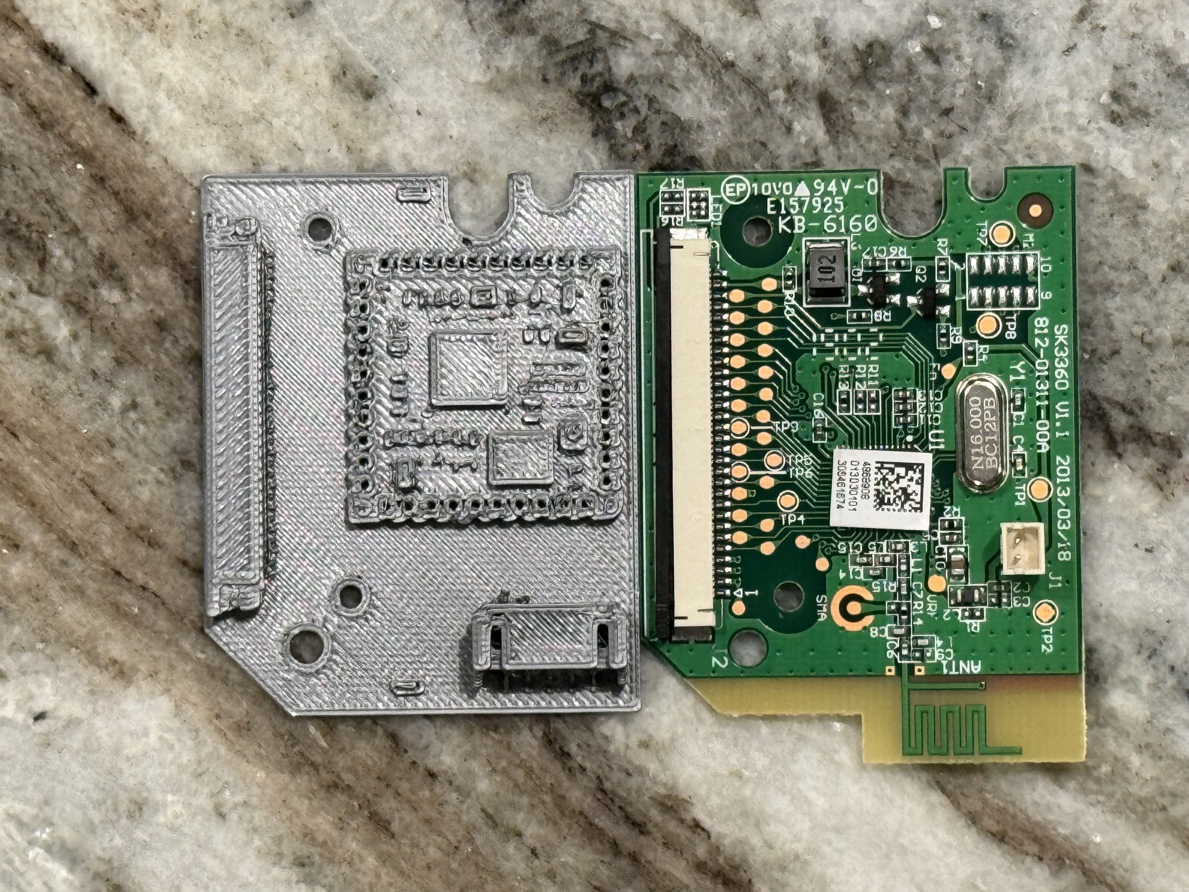
If you have a 3D printer at home and need your PCB design to fit precisely, I strongly recommend leveraging 3D print test fits to hopefully fix any physical size issues before you send the PCB to manufacturing.
Where to order?
After looking at the USB-C connector I decided that there was no way I wanted to try and hand solder it. So for the first time in a side project I decided to have a PCB fully assembled by a third party.
Needing assembly ruled out a number of PCB vendors. I used online quote tools to evaluate a number of both US and overseas vendors, and discovered that JLCPCB was less expensive than the others by a noticeable amount. They also had variants all of the parts I needed in stock, outside of the RP2040 Stamps which I had ordered direct from Sweden and were on their way to me.
I decided to order enough PCBs for five keyboards or 10 PCBs total, 5 of each PCB project (main and interface board). The component costs were relatively low, as they were all passive components (connectors, resistors, and a single button).
I used another open source add-in for KiCad to package up the artifacts for JLCPCB and uploaded them. I did receive one e-mail about the keep-out area overlapping with some of my mounting holes (not sure how that happened), but I responded and sent them a 3D image of the PCB and they moved forward with the manufacturing, placement, and assembly.
Getting the first units back from assembly
I ordered the PCBs on a Thursday and received them at my house on Tuesday. I was impressed with the turnaround time.
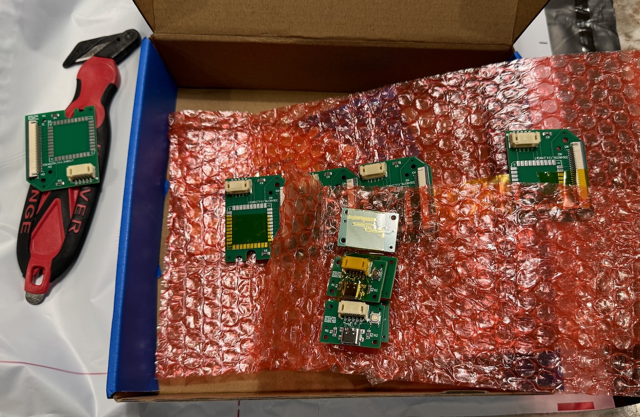
Unfortunately PostNord was not nearly as fast transporting the RP2040 Stamps, so the PCBs arrived from JLCPCB without the corresponding critical MCU component ready to solder on.
I took my disassembled Sculpt and placed my PCB in the space for the original PCB, and was ecstatic to see that it fit beautifully. I was able to easily screw it down using the original screws. As mentioned above, leverage 3D print prototyping to help your PCB fit the first time.
While I couldn’t fully assemble it, I could perform some initial testing using the PCB without the MCU installed.
Initial Testing without the RP2040 Stamp…
Leveraging experience from bring-up testing I’ve performed with EEs at work, I went through and began sequentially testing various parts of the PCB. I used a variable voltage power supply and multimeter to verify things were working as expected, and everything passed!
Here is a photo of the two PCBs sitting next to each other, ahead of me manually holding wires together while performing continuity checks.
Next to try and connect both the main board and the interface board…
Oops.
This was where I discovered (as far as I know) the only major error in my PCB design.
And it goes all the way back to the schematic. While designing it I intentionally flipped the connections between the two JST-PH connectors, thinking that they would be interfacing with a straight cable.
The issue is that the cables I intended to manufacture from two separate male JST-PH to bare wire cables had color coded ends. So they technically wouldn’t be “straight through”, instead they would be flipped along the length of the cable so that pin one on one end was the same as pin one on the other end.
I did some initial tests where I connected the two PCBs and performed some continuity testing. I got very concerned when I saw that ground on one PCB was connected to VIN on the other, and vice versa.
Everything was flipped.
I should have designed the two connectors to use identical pinouts instead of flipping the two. Oops. Thankfully, one advantage of building your own cables is you can fix mistakes like this easily by simply inverting the order when connecting the two ends.
Effectively I fixed my PCB layout issue by changing the wire connections in my custom cables.
Final Assembly
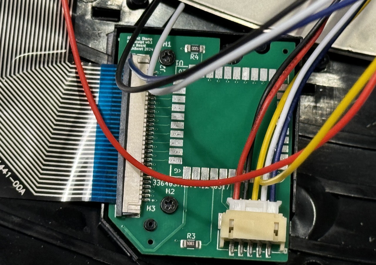
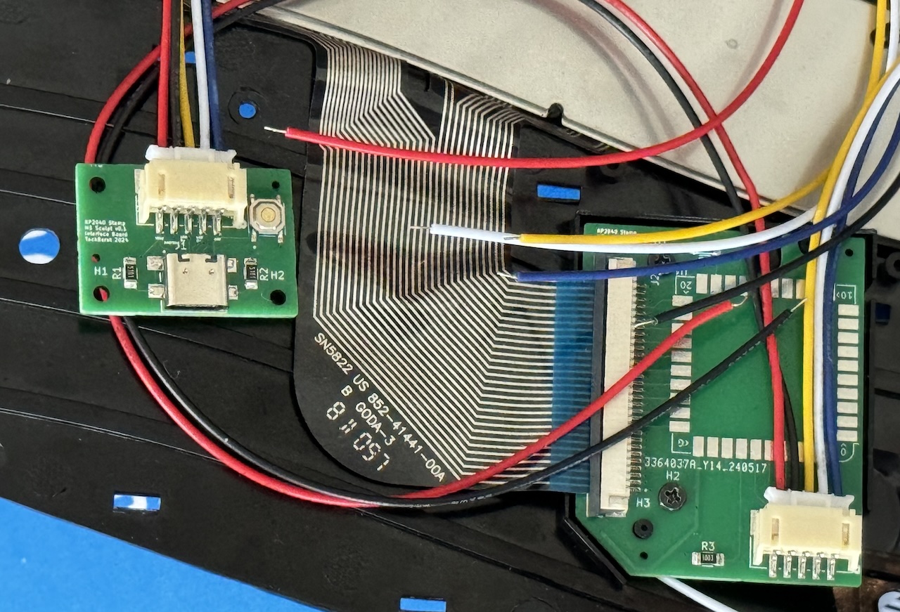
A number of days later the RP2040 Stamps arrived. After getting everything soldered together, I got the main board installed onto the keyboard, and reattached the ribbon cable.
Here you can see the cable for the interface board fed through the battery hole in the lower half of the keyboard, with the main board screwed in and the JST-PH connector installed.
After performing some multimeter continuity checks, I plugged in a USB cable to the keyboard. I was still scared I could have done something horrible, so I first did it with a power supply with a USB power meter in between to make sure that I hadn’t done something horrible that could have exploded a USB port on my laptop.
But it seemed fine, amperage readings were extremely low (as expected).
Again being incredibly cautious, I grabbed a USB-C to USB-A dock, and connected it to my laptop. I figured having the dock would act like another level of isolation between the keyboard and my MacBook.
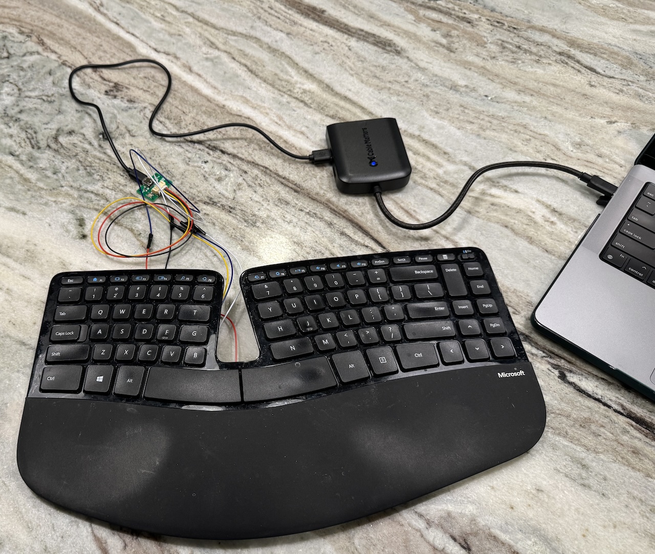
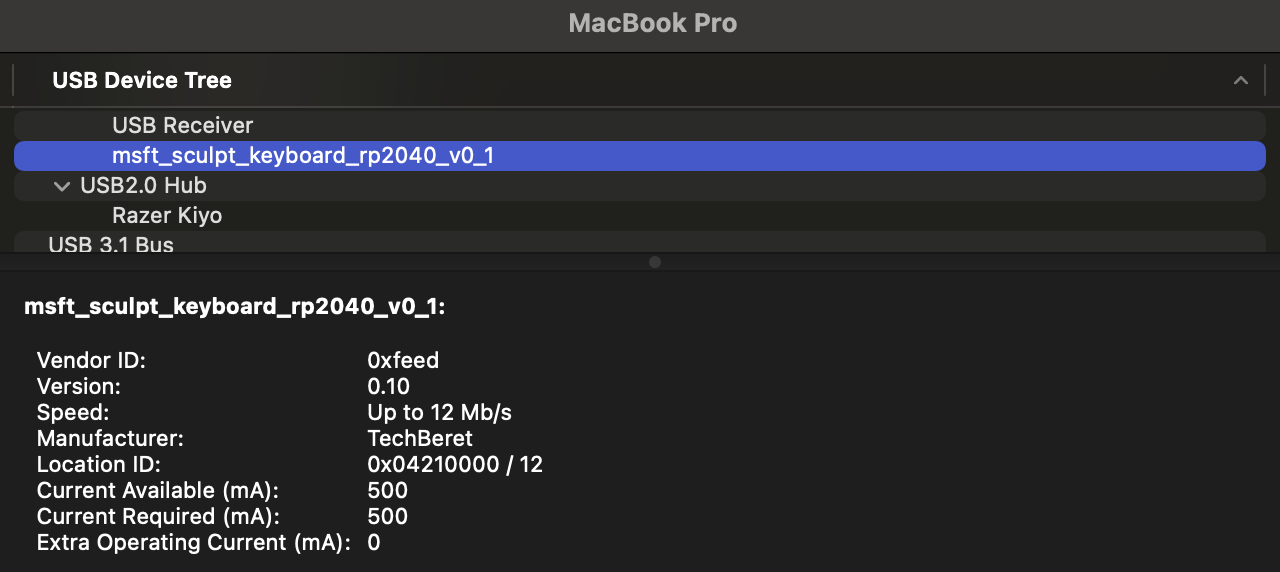
After attaching the other end of the USB-C cable to my laptop’s dock while holding BOOTSEL, the keyboard immediately appeared in Mac OS as a USB mass storage device! I then flashed the QMK firmware configuration onto the RP2040 Stamp, and held my breath while I disconnected and reconnected the keyboard.
And it worked!
After a couple minutes of adjusting the QMK keyboard layout (I leveraged another QMK EU Sculpt layout as a template) I was able to confirm every key on the keyboard was working properly.
Improving the underside of the Sculpt
Now that I had a prototype with cables that were far too long, I needed to try and make it look nicer. My objective was that everything would fit within the “battery” slot of the keyboard, and nicely expose the USB connector.
I performed some measurements of the keyboard’s battery slot using calipers and jotted them down in GoodNotes on my iPad. Then after converting my sketch into a OpenSCAD script, and test prints, and adjustment later I had something that fit extremely well into the slot, leveraging a tight friction fit.
Unfortunately during testing while the “friction fit” for the mount itself seemed to work pretty well, the moment I applied any vertical pressure on the USB cable the PCB would immediately disconnect from the mount.
So I applied a bit of hot glue holding the PCB to the mount.
Hot glue is an awesome tool in any hardware hacker’s toolbox as it is typically easily removable, doesn’t damage stuff, doesn’t get all that hot, and does a decent job holding stuff together.
Next I trimmed the very long cables between the two PCBs, and used some solder seal heat shrink for the first time to join the two cables.
I now had a keyboard I was even more proud of.
A keyboard I’m loving
Virtually all of this was written on one of my converted keyboards, outside of some writing on my MacBook while traveling. Overall I’m extremely happy with how the project turned out.
I updated my initial QMK config to support the Fn switch in the top right of the keyboard, and added in support for the multimedia keys I cared about. So things like volume up, volume down, mute, etc now work 😃.
It also feels awesome to see TechBeret listed as the manufacturer in Mac OS’s System Information panel.
As with any side project, I do have a couple things I would improve with a second revision, starting with supporting both LEDs, requiring either a voltage pump or an inverted voltage source. I also want to make another mount revision which covers up the solder heat shrink connections for better aesthetics. Finally I have a bit of a crazy idea for a gen 2 I don’t really want to spoil yet, but I have a new SoC dev kit sitting in my home office waiting for me to have some time to experiment.
Appendix A: The cost
As I mentioned in the first post, I either used old keyboards that had previously died on me or cheap dongle-less ones off eBay, so I’ll estimate roughly $30 for each keyboard, including shipping.
It cost me just under $70 (including tax and shipping) to manufacture the 10 PCBs (5 primary and 5 interface boards) using JLCPCB, which is remarkably cheap considering I needed to use the more expensive manufacturing options due to the USB-C connector’s tiny connections.
The RP2040 Stamp was $72 for quantity 6 RP2040 Stamps ($12/piece), and an additional $19 for shipping.
I did use a number of miscellaneous parts, including solder, solder heat shrink, and JST-PH cables from Amazon, so I’ll add a dollar for each board for those miscellaneous parts.
So the overall cost is roughly $60 per keyboard. If you have a dongle-less or dongle-broken Sculpt lying around it is only $30 in parts. Not bad at all. And it could be likely reduced noticeably if I didn’t use the RP2040 Stamp, but instead had those components on my primary PCB.
Appendix B: Project Source Code Links
Note that I have not yet fixed the inverted cable problem, but I still wanted to make sure to open source this project fully for anyone else who wants to try it out. Note that the QMK is currently a fork off of an earlier version, as I haven’t converted mine to use the new format. Eventually I’d like to merge my keyboard into mainline QMK…
Hardware Projects
The following repository contains both the primary and interface board KiCad projects, along with the OpenSCAD soldering template and board interface mount project. I’ll probably write a future blog post about the soldering template.
MSFT Sculpt RP2040 Stamp HW Github Project
Fork of QMK with configuration
The following repository is a fork of QMK. I built the first prototype a while ago, and would need to make some changes to the project for it to be compatible with the newer revisions of QMK, so currently it is off a fork.
QMK Fork with Sculpt RP2040 Config
Thanks for reading!
I hope this was at least interesting. Make sure to let me know via Mastodon if you take on your own Sculpt PCB project! Special thanks to all the people who worked on Sculpt PCB projects previous to me, I was able to leverage your hard work in getting my project to this point.
Good luck, and keep hardware hacking!
NOTE: All Amazon links above are affiliate links, and if you buy through links on the site I may earn an affiliate commission.